
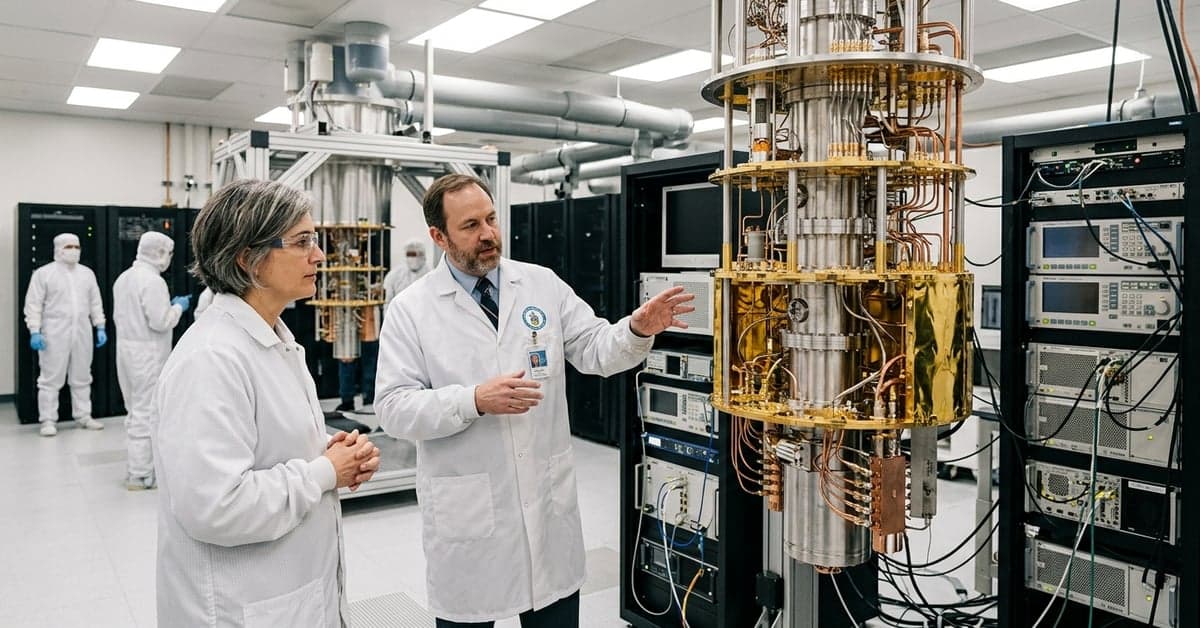
On September 16, 2026, IBM said its subsidiary Anderon finalized an agreement with the U.S. Department of Commerce for a $1 billion CHIPS award to speed research and development for a U.S.-based pure-play quantum foundry, according to the IBM Newsroom. The size, scope, and the phrase “pure-play foundry” point to a shift: quantum hardware is edging from lab prototypes toward industrial process control and shared manufacturing access.
Why a $1B bet on the IBM quantum foundry matters
The CHIPS and Science Act is best known for bolstering semiconductor fabs. It also sets aside large sums for R&D infrastructure that turns research into manufacturable tech. The CHIPS Program Office has outlined centers to bridge basic science and production. A $1 billion award attached to a single initiative sends a clear market signal: Washington wants a domestic quantum hardware base with repeatable processes, supply chain depth, and workforce scale.
IBM’s framing around a pure-play model matters. In chips, the fabless–foundry split let small design houses ship at scale by renting time on shared fabs. That unbundling fueled an explosion of innovation. The Semiconductor Industry Association credits the model with broadening access and competition. A comparable structure for quantum could let startups, universities, and national labs manufacture devices without owning their own expensive, specialized tooling.
For the U.S. government, a shared manufacturing hub also concentrates security, export control compliance, and process assurance in a small number of audited facilities rather than a scatter of bespoke labs. That simplifies oversight and builds resilience into the hardware pipeline.
How a pure-play quantum foundry changes access
Quantum devices are still diverse. Superconducting, trapped-ion, neutral-atom, photonic, and spin qubits all demand different materials and tools. A pure-play quantum foundry won’t erase that fragmentation, but it can standardize the layers around device build and test that most pathways share: cleanroom process controls, packaging, cryogenic test, metrology, and documentation. That consistency is the on-ramp early teams often lack.
According to Quantum.gov, federal strategy has moved from funding isolated testbeds to knitting a national ecosystem. A shared, U.S.-based foundry is the institutional version of that idea. If the facility offers structured design kits, reserved runs, and published process windows, more players can ship working hardware. If it also supports foundry-style multi-project wafers or batch runs for different device types, costs drop and iteration speeds up.
Open access doesn’t mean open season. Expect tiered access, security reviews, and priority scheduling tied to federal missions. But compared with today’s bespoke routes, that’s still a wider door. For startups, a credible foundry can make the difference between a pitch deck and a shipping prototype.
Who benefits first—and who has to adapt
Three groups stand to gain early. First, small companies building sensors, clocks, and communications hardware that use quantum effects but don’t need thousands of qubits. They get manufacturing discipline sooner. Second, university and national lab teams with grant-backed device designs that require a cleanroom ladder higher than campus tools can offer. Third, defense and aerospace integrators who need trusted, traceable quantum components for systems work.
Large, vertically integrated quantum vendors may need to adapt. A neutral facility that others can book reduces the advantage of owning every step in-house. The trade-off: even incumbents get a second source for overflow, process comparison, or specialty steps they don’t want to invest in.
The broader supply chain benefits if the foundry publishes specifications for materials, cryo-packaging interfaces, and test fixtures. Shared specs pull in suppliers that have been hesitant to retool for a fragmented market. The Quantum Economic Development Consortium (QED-C) has long argued that standard interfaces and common metrics are preconditions for scale; a foundry can anchor both.
What to watch next for the IBM quantum foundry
Today’s announcement leaves key questions. Governance comes first: who controls the queue, and what share of capacity is tied to federal missions versus commercial runs? Pricing matters for startups. So do IP terms, design kit maturity, and whether multi-tenant runs are part of the plan. According to the CHIPS R&D guidance, awards are tied to milestones and public benefit; watch for a published roadmap with process targets and access policies.
Technical scope is the second wildcard. Will the facility focus on one device family at first, or offer a menu of processes with clear process design kits? In semiconductors, the foundry model took off when a stable process node and PDK let designers predict yields. Quantum needs its own version of that stability, even if early runs are lower yield and higher variance.
Third, regional links. Workforce pipelines, supplier parks, and logistics around cryogenic equipment do not spring up overnight. Expect partnerships with universities and community colleges near the site to train technicians. National initiatives point the way; the National Academies highlights technician shortages as a barrier to growth. The presence of a shared facility often catalyzes that training.
Finally, transparency. The promise of the IBM quantum foundry model is access and repeatability. That promise is only as strong as the process data, failure analysis, and yield reports the operator is willing to share with customers. Investors and program managers should look for regular, audit-ready reporting tied to CHIPS milestones.
In short, the IBM quantum foundry announcement is less about one lab’s next device and more about industrial plumbing: shared tools, shared rules, and a way for many actors to build. If it delivers on the pure-play vision, it could accelerate a domestic quantum hardware market that is bigger, more open, and less fragile than today’s lab-by-lab patchwork. For more on this, see reuters.com and bloomberg.com and nytimes.com.
Related reading: Federated Learning • Quantization • Machine Learning