On June 17, 2026, Nature reported a prototype vision system that embeds core computer‑vision operations into an optical metasurface, delivering real‑time perception on the sensor itself. The News & Views piece describes a general‑purpose approach: light passing through a patterned material performs the first steps of seeing, before a chip lifts a finger. That places the work squarely in the machine learning latest conversation for on‑device AI.
Why this lands in the machine learning latest spotlight
Nature’s summary says the metasurface handles fundamental vision operations optically, enabling accurate, real‑time results across multiple tasks with low energy use (Nature, June 17, 2026). Most optical systems demonstrated over the past decade have been either task‑specific or too brittle outside lab conditions. The claim of general‑purpose capability, paired with real‑time performance, hints at a shift: compute is migrating into the camera stack, not just sitting behind it.
The timing matters. Edge models have grown more capable, but batteries and thermals still set hard limits in phones, glasses, and drones. If the lens itself can do part of the math, downstream silicon can shrink, idle more often, or run cooler. That’s the draw here, and it explains the excitement around metasurfaces and in‑sensor computing in academic circles and industry alike.
How an optical metasurface moves compute into the sensor
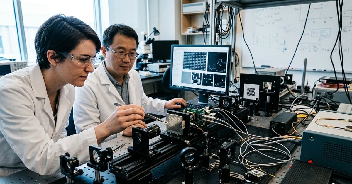
A metasurface is a thin layer etched with subwavelength features that shape light in programmable ways. By designing those features, researchers can make the material act like a bank of optical filters, approximating convolutional operations as light streams through. In effect, some of the linear algebra behind vision models gets offloaded to physics. Reviews of optical and photonic neural networks have charted this direction for years, showing how diffraction and interference can implement layers of a network at the speed of light (Nature Photonics review).
Earlier demonstrations, such as diffractive deep neural networks, established that stacked optical elements can perform classification and imaging tasks without electronics in the loop for the first pass (Science, 2018). The new work highlighted by Nature goes after breadth. Instead of optimizing optics for one dataset or one label set, the reported prototype folds “core computer‑vision operations” into a single planar structure. A conventional image sensor and a modest processor then complete the pipeline.
That split—preprocess in photons, postprocess in electrons—could prove practical. Optical layers handle the heavy, repetitive filtering with zero dynamic power and near‑zero latency. Electronics take on nonlinearities, memory, and control logic where programmability is key. If the metasurface can be manufactured reliably and paired with standard sensors, it fits today’s supply chains rather than inventing new ones from scratch.
What the latest in machine learning can’t do on silicon alone
Even efficient neural accelerators fight a three‑headed constraint: data movement, heat, and idle power. Moving pixels from the sensor to DRAM and back burns more energy than many arithmetic operations. Optical preprocessing trims that bandwidth at the source. It also cuts latency for always‑on perception loops, where shaving milliseconds helps stabilize a drone, reduce camera shutter lag, or keep AR overlays from drifting.
Power is the other lever. Analyses of AI’s energy appetite keep pointing to growing costs per user as models and use time scale up (Joule, 2019). On‑sensor filtering lowers the energy per frame before silicon touches the data. That matters for smart glasses and earbuds, where every milliwatt shortens run time and heats skin. It also matters for privacy. If raw frames never leave the module, and only features pass downstream, less sensitive data needs to be stored or transmitted.
None of this works if the optics are brittle. Real cameras face temperature swings, vibration, and manufacturing variation. The reason the Nature report stands out is the “general‑purpose” claim joined with a prototype tested across diverse tasks, not just a cherry‑picked benchmark. If that holds under independent replication, the practical window widens beyond labs and demo booths.
Limits, open questions, and why the bet is on meta‑optics
Programmability is the first question. Fixed metasurfaces can be blazingly efficient but hard to retarget. Tunable meta‑optics exist, using materials or MEMS to change phase profiles, but they add complexity and cost. Reviews of metasurface engineering lay out the trade‑offs between static and reconfigurable designs, and the fabrication tolerances needed for volume production (Nature Photonics, metasurfaces review).
Calibration is next. Any optical layer that computes is also an optical layer that can drift. The electronics chain will need self‑test routines and learnable compensation to handle temperature, aging, and unit‑to‑unit variance. Tooling must mature as well. Photonics‑aware model training, differentiable optics, and co‑design flows have to become routine for camera vendors and chip teams. That means new software stacks bridging optics, sensor design, and ML frameworks.
Finally, fairness and safety rules don’t vanish just because photons did some work upfront. If a metasurface bakes in a biased filter bank, its errors are harder to inspect. Nature’s coverage of health chatbots earlier in June underscored how system‑level choices shape outcomes. The same lesson applies to cameras that pre‑decide what reaches silicon. Documentation and content provenance tags could help track how and where in‑sensor processing was used, especially in security and public‑space deployments.
What to watch next for on‑device vision
Short term, expect hybrid modules that pair a task‑tuned metasurface with a compact CNN or transformer head. The optical front end trims bandwidth and noise; the silicon back end handles control, fusion, and updates. If camera makers can drop such modules into existing sockets, phones and drones could see faster autofocus, steadier video, and better low‑light capture without big battery hits.
Medium term, the open questions are playbooks and standards. How should vendors report performance when part of the model is etched into glass? What’s the equivalent of a model card for a meta‑optic? And how do developers debug a system where gradients pass through physics? Researchers have started to answer pieces of this with co‑design toolchains and photonics simulators, but shipping products need repeatable tests and shared metrics.
Longer term, reconfigurable meta‑optics would unlock wider use. A single camera that can switch between motion detection, depth cues, and low‑light enhancement without a lens swap would change how devices sense the world. Work on tunable metasurfaces points that way, though materials and control circuits still limit speed and range (IEEE Spectrum on metasurfaces).
Nature’s June 17 report doesn’t claim to end the need for silicon accelerators. It does point to a credible path for shifting the first, costly steps of seeing into the optics. That’s a machine learning latest story worth tracking, because it touches the physics, the software, and the supply chain at once. If it holds, your next phone could feel faster and cooler, not because the chip got bigger, but because the lens got smarter. For more on this, see bloomberg.com and nytimes.com.
Related reading: Federated Learning • Quantization • Machine Learning